Tactic-toe (Hardware)
Please first see the overview article to learn about tactic-toe
Inspirations
One of the projects that I have always wanted to do is to make my own PCB business card.
I’ve been inspired by the designs online that people share. Typically, each of them have its own gimmicks, and they come in varying quality. Some are superb, but some are what people online (not me) call as “E-Waste”.
Design Examples
There are just so many designs out there but here are few of my favourites:
- Stylophone (by Mitxela)
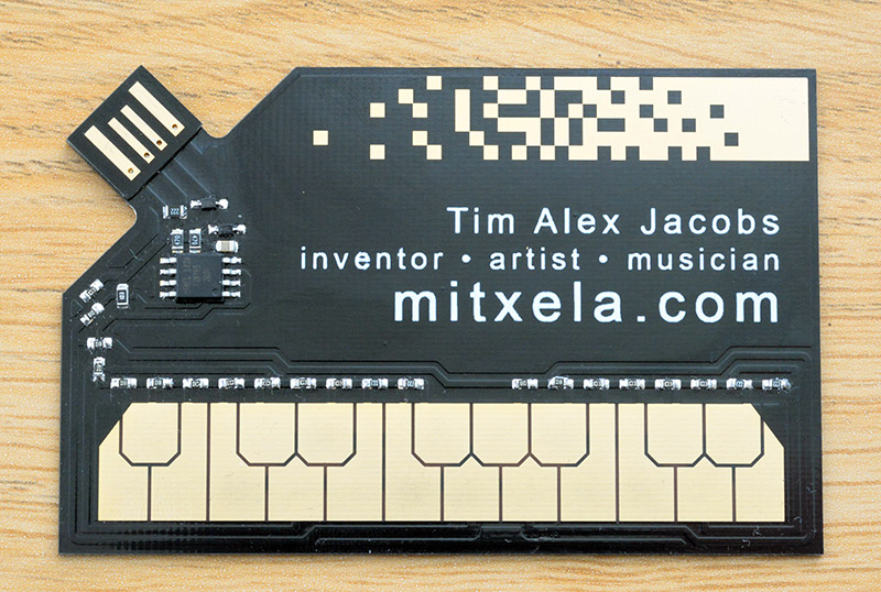
This might be the earliest design I saw on YouTube by mitxela. It’s a stylophone PCB which is pretty cool. Its essentially one of the revolutionary ones because it has a USB-A as part of the PCB itself to make it very thin.
- Fluid Simulator (by Nick Johnson)

This is an example where a simple idea if executed properly can be awesome. I have seen many attempts at making a similar idea but this time its much higher resolution and such at a smooth fps which just tickles your brain right. Its one of the more recent designs I saw and definitely one of the most complex software-wise. Plus, it also has a female type-C connector as a part of the PCB.
- Persistence of Vision (by Ben Eater)
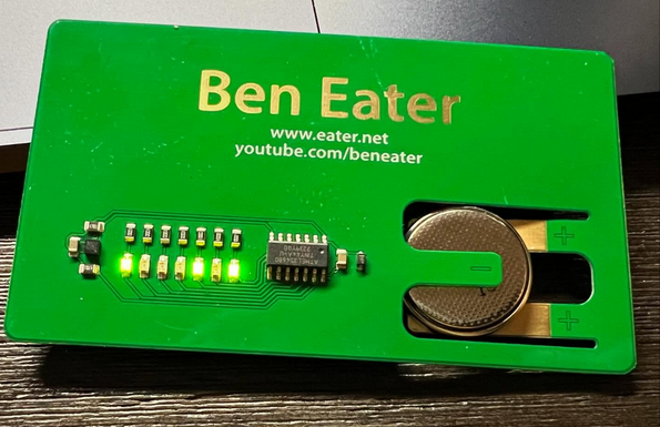
Image taken from instagram
This one is from my favourite ASMR electronics YouTuber Ben Eater. Its so simple yet one of the coolest one in my opinion. It acts like a persistence of vision wand, when you to shake the card, the LED displays text of his name. The onboard IMU and MCU to controls the LED timing when shaken. It also has a very creative battery holder which make use of the PCB’s flexibility.
- Other designs
There are other designs that I’m not really a fan of which are quite common.
- NFC cards: Its cool and complex to tune the antenna, but I think it doesn’t fully make use of a PCB when you can get NFC cards cheaply pretty common nowadays.
- Not business card sized or too thick: Some of these are genuinely really cool, but it just doesn’t fit the theme of a business card.
- PCB without any components: Some designs sometimes just have a ruler and printed graphics. Sure it looks nice, but again it doesn’t fully make use of the PCB medium.
How good the design is depends on what you are actually trying to do with it. At the end of the day having one is cooler than not having one. Plus, it is a great learning opportunity.
Requirements
Now that we have looked at some inspirations. I have a few requirements for my own design.
- As thin as possible + credit card sized
It is not really a business card if it is too thick or in a different size. So for this as a minimum it has to fit inside a typical wallet. This requirement alone rules out a lot of typical components including through hole components and buttons.
- Cheap and Simple
Cost is a huge consideration. Since I’m planning to give it to people, I will be making quite a few of them and the cheaper they are the better. This indirectly means as little components as possible (within reason).
- Runs the perfect Tactic-toe AI
As part of the overall goal of the project, the microcontroller used must be capable of running the AI locally. This shouldn’t be much of an issue since most MCU nowadays are fast enough, but as I later realize, flash size might be an issue.
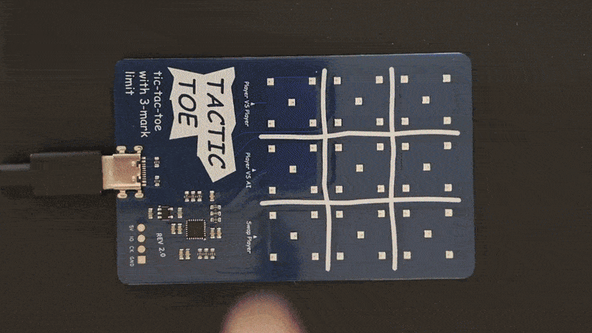
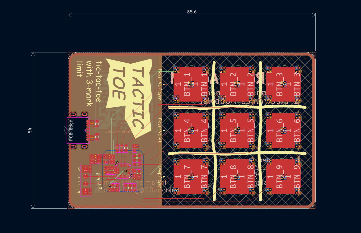
My Design Idea
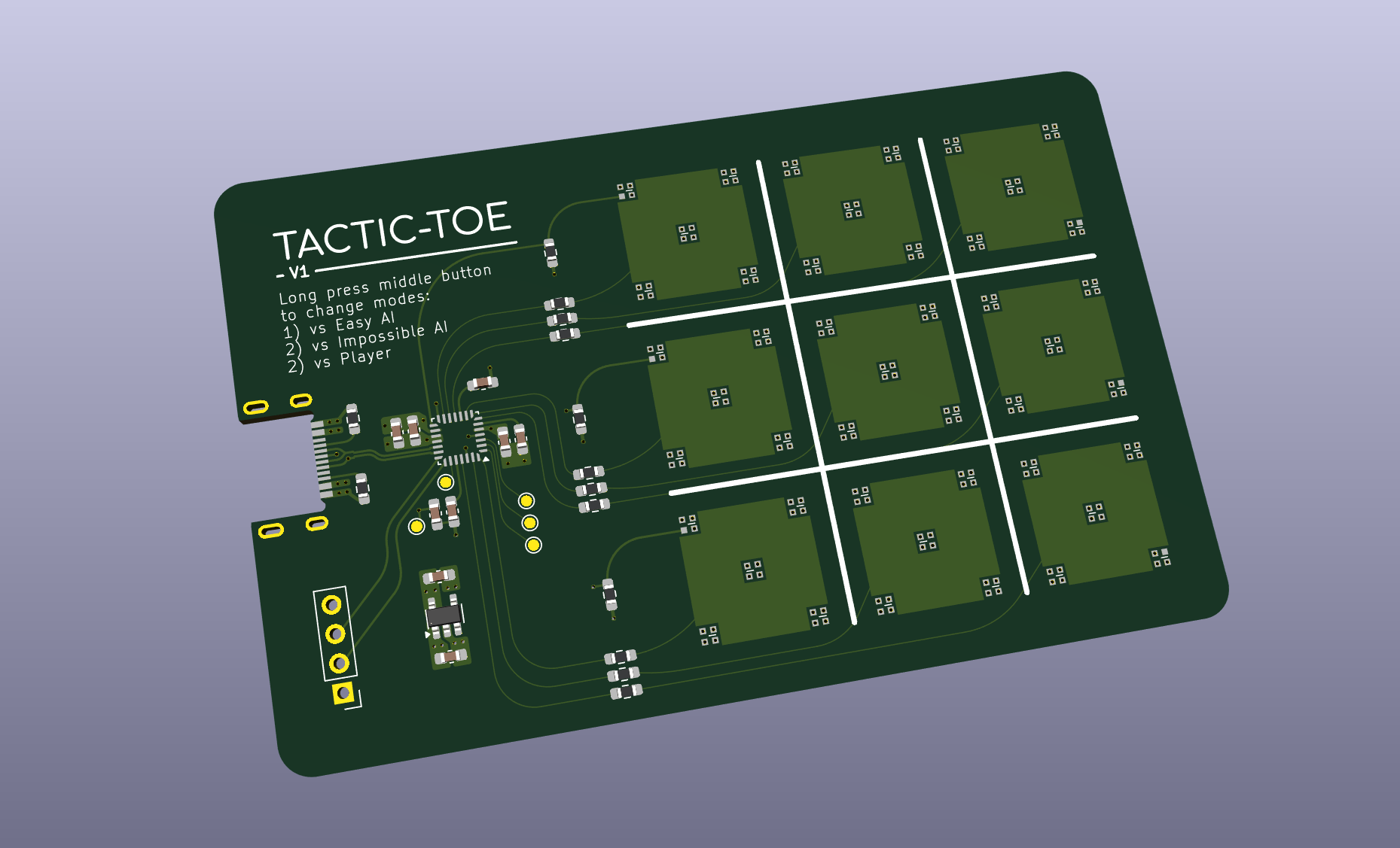
Roughly, this is what I came up with:
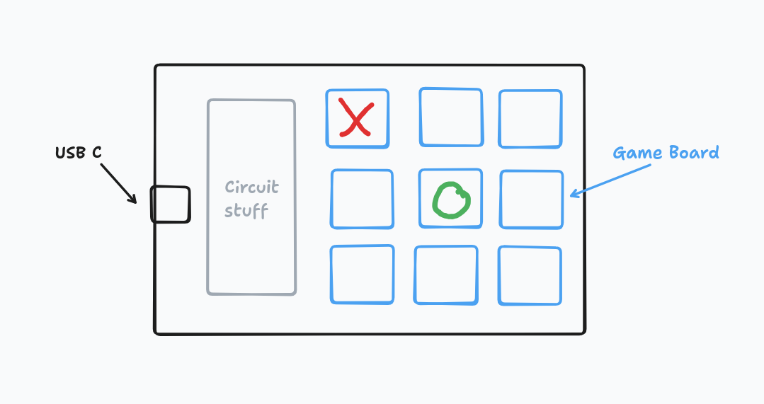
On the other side of the PCB, it has the graphics for my contact-details and a QR code to my website.
The two key choice with this design - how do player interface with the game and how does the game board display the board.
First, player interface. Buttons are a no-go for me since its quite thick and makes the PCB slightly uneven. There are super thin buttons, but they are rather ugly in my opinion. A much better alternative is touch sensors that are built in the PCB layer. This comes at a more complex trace routing design but its worth it for a cleaner look.
Second, board display. Definitely will use LEDs for lower cost. But how would you indicate X or an O? You could use different colours or different shapes.
A typical LED would require one GPIO from the MCU to control ON/OFF. Assuming the least amount of LEDs, i.e. 2 LEDs per square, one for each colour player, you would need 9x2=18 GPIO pins. Plus, with 9 touch inputs, then you would need an MCU with larger package which typically comes at a higher cost. This is not even considering if the MCU can sink/source enough current for all LEDs.
Eventually, I settled with 5 RGB LEDs in X shape config per square:
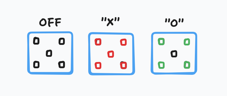
At least that was the plan. After getting showing the version 1 to people and getting feedback, I ended up just using the X with different colour to differentiate X and O.
Using addressable RGBs has the advantage of much easier routing as each RGB LED has its own built-in controller. What that means is that each LED is controlled using a single asynchronous data line (like UART), and it can also be daisy-chained. Plus, each LED can be powered directly from 5V without any current limiting resistor. Brightness and colour can easily be changed using the data signal.
To keep costs lower, and not make the PCB too thick, I decided not to have any battery onboard. Instead, the PCB has to be powered using 5V USB. Having a battery requires an extra DC-DC converter circuitry and potentially charging circuitry if rechargeable battery is used. I think its worth the tradeoff especially since power banks are pretty cheap nowadays to make it portable if needed.
Component Selection
For the cheapest generic components bought in bulk, LCSC is the place to go. AliExpress can offer better price but navigating the amount of scams and counterfeit components is just not worth it. So, all the components are surveyed on LCSC for this project.
RGB LEDs
This will be the most expensive part of this project due to the amount required. They are not as cheap as normal LEDs. So, for this, I sorted by price on LCSC and looked at its size, where smaller is better but not too small otherwise it will be impossible to solder by hand.
In the first revision I have opted for OPSCO Optoelectronics SK6805-EC15:
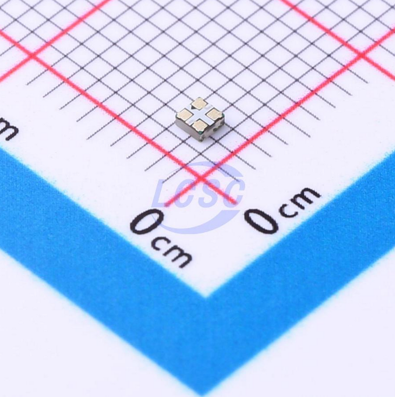
SK6805 is the internal RGB LED controller, and EC15 (1.5mm x 1.5mm) is the package size. This was actually not the cheapest at $0.0605 each as I was not very familiar with RGB LEDs at the time and there were lots of confusing info online, so I just went with it.
It’s super tiny with the pins underneath which makes fixing soldering mistakes 100x much harder than it should, and so in the next version I swapped it out with a much cheaper XINGLIGHT XL-1615RGBC-2812B-S:
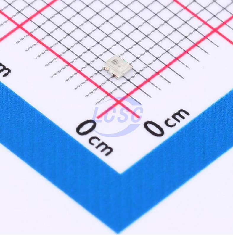
It’s the cheapest RGB LED at $0.0236 with a well known controller (2812B) and a small enough package. It has a different RGB controller with a slightly different data signal timings but its similar enough to sk6805 in which a simple change in software can make it compatible. A more common variant of this LED with the same controller is WS2812 which are more common with addressable LED strips with much higher brightness.
Capacitive Touch Sensor
As discussed, I wanted a touch sensor. There are many ways to achieve this, but the most common way to implement directly on a PCB is capacitive touch sensor. To put simply, a capacitor is formed with two plates placed close together. The way the sensor works, the copper on the PCB forms one side of the capacitor and your finger becomes the other plate, and depending on the distance of your finger to the copper, it varies the capacitor value in the order of picofarads (pF).
Then to measure the capacitance, there are many methods to do so. There are even plenty of dedicated touch controller ICs. However, in an attempt to make it as simple as possible, I opted to use STM32’s hardware touch sensor peripheral. This means that I have to look for STM32 that has this peripheral as not all of them has it.
TSC or Touch Sensing Controller is STM32’s implementation of hardware touch sensing peripheral. The way TSC works, it charges the sensor capacitor, and then uses it to charge a sampling capacitor. Since the sampling capacitor are much larger than the sensor capacitor, it will take multiple cycles to charge the sampling capacitor. Then, depending on how many cycles it took to charge the sampling capacitor, you can relatively measure the capacitance of the sensor capacitor, i.e. if a finger is close to the sensor.
The equivalent circuit is shown below:
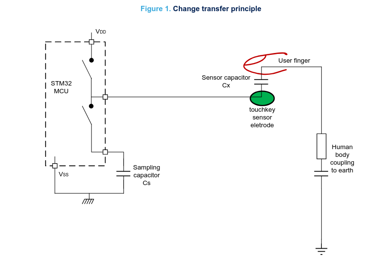
Image taken from STM32 wiki
Different microcontrollers brands have their own implementation of measuring capacitance and I read somewhere that Microchip has a better implementation, but I couldn’t find where I saw it. Its just worth mentioning because there are other methods of measuring capacitance and some might be better than the other depending on the application.
Microcontroller
The second-highest cost component is the MCU. To reduce the complexity of this project I’ve opted to use STM32 that I am already quite familiar with. So, I filtered STM32 series with hardware TSC and sort by price. The cheapest one I found is STM32F042G6U6TR for $0.8811 each.
It uses ARM Cortex-M0 with 48MHz clock speed. Plenty for this application. It also comes in UFQFN-28 package which is solder-able with hot air or even hand solder. However, that also means we are quite limited in usable GPIO pins. Luckily, it has just enough pins to make this design possible.
What’s unfortunate is the ROM size, which is only 32 KB Flash. This is plenty for most application, but it does limit what I can do and became a limitation in firmware when implementing the AI. Will be explained more in firmware article.
Linear Regulator and Other Passives
Since the STM32 runs on 3.3V, a linear regulator is needed to step down the USB 5V to 3.3V. We don’t need any fancy feature or the best noise performance, so the cheapest Linear Regulator from Ti was chosen (TLV74033PDBVR) in the standard SOT-23 package.
There are no requirements for the passives (resistor and capacitor), so the cheapest generic component with appropriate voltage rating are selected. 0603 package size are chosen for all since its small enough but also solder-able by hand in case needed fixing. However, there is a recommendation by application note AN4310 to use specialized NPO or C0G for the best touch sensing sensitivity, but as I found, typical X7R MLCC are good enough for this application.
Version 1
For this first version, I played it safe to get at least something working since this is the first time I designed a touch sensor PCB. STM32 provides a lot of different application notes to help with the design of the touch sensor. However, I realised that A lot of the application notes is for high sensitivity or off-board touch sensing application.
I found the most useful application note for the design of touch sensor on a PCB is AN4312. It provides a lot of guidelines on how the sensor should be routed and some general dimensions to be followed. Many of the values and guidelines ties back to fundamentally how to maximize the capacitance on the touchpad while minimizing capacitance of the traces to the MCU.
Layer Stack-up
It is practically impossible to route this board with only 2 layers knowing we need GND, 5V, Data IN/OUT on every corner of the LEDs. You might be able to, but it is not worth my time to optimize it to that level unless I have to. 4 Layers are the way to go, especially now the price are not that expensive compared to 2 layer boards with JLCPCB which is the service I will be using to manufacture the PCBs.
For the stack-up, unlike your typical PCB design where you want signals to be as close to ground, the opposite is required for the touch sensing pads. This is because you don’t want the majority of the capacitance formed by the coupling between the ground plane and touchpad. If so, your finger will barely change the capacitance, and it will be much difficult to detect the change in capacitance.
However, having no plane at all can introduce noise susceptibility to the sensor. That’s why, it is recommended to have thinly hatched plane underneath the touch sensors to balance between noise and sensitivity of the sensor. The GND plane is shown below:
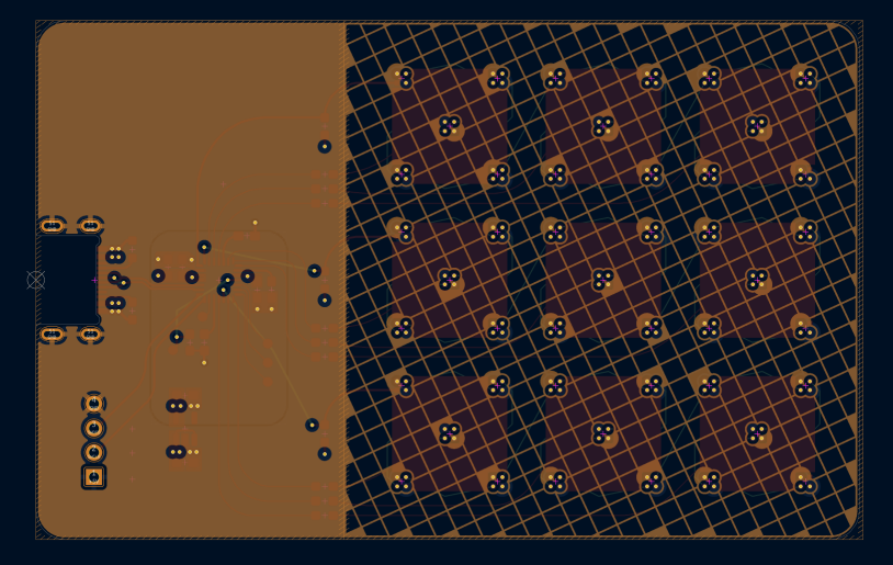
Therefore, in the first version, the layer stack-up is:
- Signal Layer (Touch Sensors)
- Signal Layer (LED data signal routing)
- GND Plane
- +5V Plane
The touch sensors are distanced from the planes. The GND and 5V planes are closely placed to increase inter-plane capacitance and reduce impedance.
Having 5V at the bottom with exposed copper QR code graphic was not a good idea and the 5V and GND was swapped in the second version.
Touch sensor with RGB Routing
As you can imagine, the capacitive touch sensor pads which are typically in the range of pF, can be very sensitive to noise. This is a huge a problem when you have a fast digital signal for the RGB LEDs that are very close to the pads. To minimize the crosstalk between the capacitive sensor and the LED data signal, the smallest trace width was used, and I optimized it to have minimal area overlapping between the two copper surfaces since I am routing them in different layers:
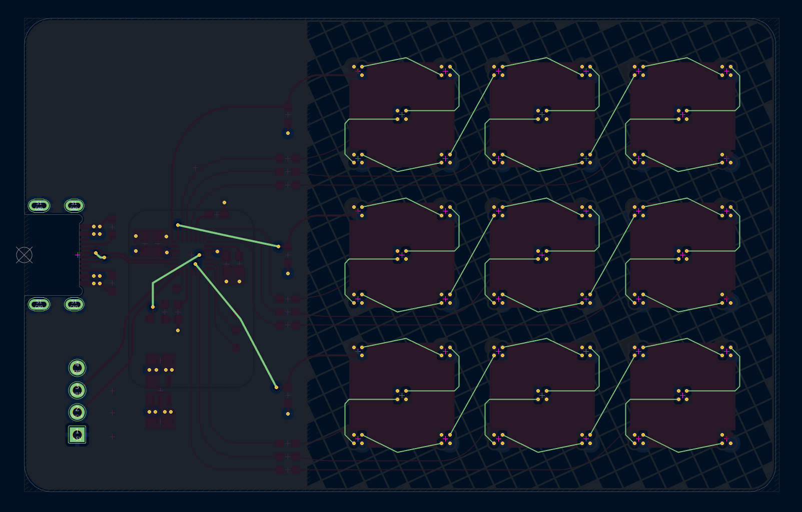
The way the sensor and LED is connected is by having three identical rows of sensors and routing. The three rows each has its own LED signal channel connected in daisy-chain configuration. So then it becomes this weird shape which I think is pretty cool. Though you can’t really see it in the actual PCB because it is embedded in the second layer.
Graphics
The back of the card has my contact details with a QR code to my website. Silkscreen are pretty plain, a much cooler looking is reflective copper, so you can get like 2 tone colour for PCB graphics. To do this you need to create a custom shape on the copper Mask layer which are typically used to define exposed copper pads. You can do this very easily in KiCad using Image Converter tool and selecting F.Mask layer in the output.
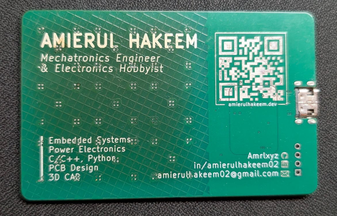
It doesn’t look very different on camera since in the first version it uses lead-free HASL finish, so it looks silvery-ish. On the second (final) version I used ENIG (gold plating) so that it looks much nicer and contrasts the normal white text.
Another big thing to notice is that the silkscreen around vias were removed as part of the manufacturing process because I chose the option of plugged via rather than the more expensive ‘filled & capped’ vias. The former is typically used for via-in-pad for a flat surface finish.
Result
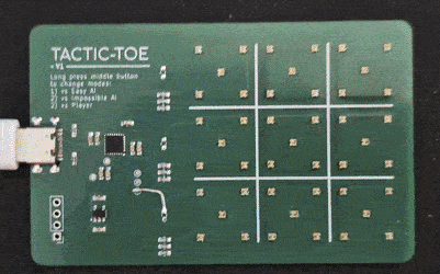
The unspoken rule of any PCB design is never assume that the first version will work. Indeed, I made quite a few mistakes in the first design. Though luckily I did add quite a few test points and after some bodging I did manage to make it work.
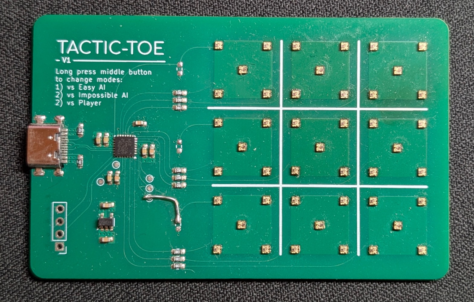
The board was a bit dusty when I took the picture. As you can probably see from the dark marks on the board, that shows how much the board has been ‘cooked’ in order for me properly solder it. The LEDs were a pain to solder even with a hotplate and hot air gun. I spent almost a whole day just to solder one board, and even that was pretty lucky because I failed to solder any other V1 boards completely.
In my design, I used via-in-pad for the RGB LEDs to make the routing much simpler with less footprint area. This comes at the downside that the vias could suck in solder paste when soldering the SMD pads. I wasn’t expecting this to be a huge issue with manual soldering as I can fill them in manually before starting the soldering process. Even with that extra step, some vias are not fully filled, so it sucked the solder resulting in uneven and unconnected solder joints.
To fix this, its simple, just use plugged & capped via if you are doing via in pad for SMD components. Lesson learnt
Version 2
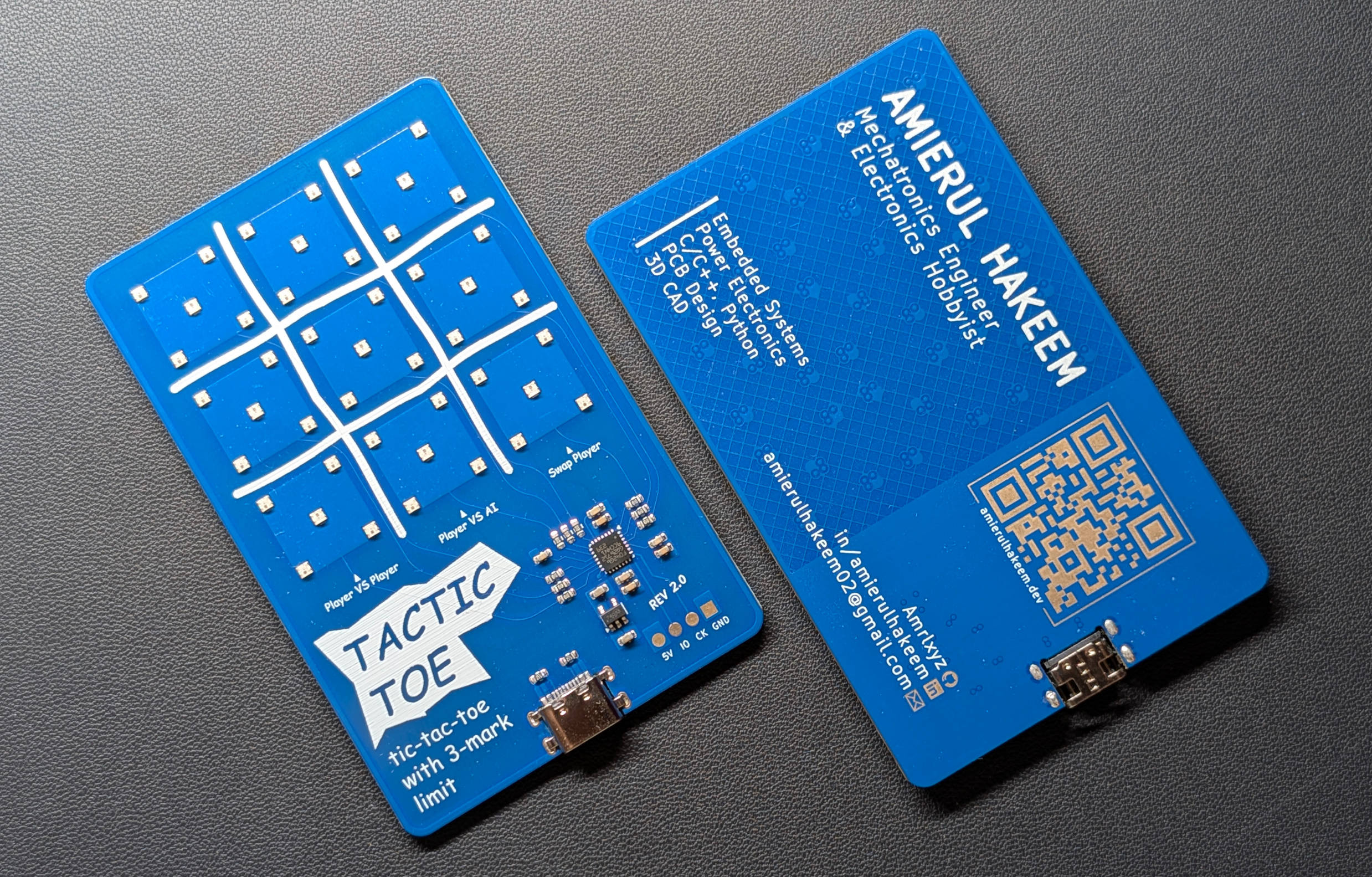
Version 2 includes the changes mentioned previously with other minor changes:
In terms of the design:
- Replaced RGB LEDs
- Swapped GND and +5V Planes
- Fixed wrong PWM pin fault in Version 1
- Remade top PCB graphics
- Other minor fixes
Apart from that, the design is practically the same.
Manufacturing Options
At the time Summer was almost ending, I decided I have to finish the project quickly. I don’t have enough time to make another prototype version. So, I took a gamble and make the changes and fully commit to manufacture the final version (V2) without testing it first.
Considering that I took almost one whole day to solder just one board, I thought it might just be better that for this final version, I should try out JLCPCB Assembly service. Although, it will be a bit more expensive, it would save me so much time and the quality of solder will be much more consistent especially since I will be giving them away.
Pro Tip: To keep costs low, make sure to use basic components on JLCPCB assembly otherwise there will be extra setup costs. There are also some components considered difficult to assemble which will add even more fee on top. One example is the USB-C connector I used. So, I decided to solder them on my own.
Fun fact: LCSC and JLCPCB are kind of the same company so the components available on LCSC are likely to be also available for JLCPCB assembly service.
I also wanted to get the more expensive manufacturing options, ENIG finish, Epoxy Filled and Capped Vias, it will further add more to the cost. With all these in mind, I can’t mess up this final version otherwise it will all go to waste.
After placing the order and waiting for 2 weeks anxiously, it arrived. I soldered on the USB-C connector, and it just works. I was so happy that it worked and how clean looking it turned out. The soldering job is far better than what I can do with my tools (obviously).
Total Costs
Here comes one of the most frequently asked question when I showed the PCB to people:
How much does it cost to make one?
Before I get into the cost, I have to address something:
At the start I mentioned that cost was one of the biggest factors but at the end, I chose the expensive way of manufacturing the boards. Sure, I could spend less money by optimizing the board for the lowest cost possible and soldering each board myself, but that will take significantly more time. Plus, I recently got some extra money from my summer internship, so I call the extra costs as investment for myself.
Now that’s settled,
The total cost is: £213.09 + £56.89 (tax) = £270 for 50 boards, which is £5.4 per board. Yeah, was not cheap. I made a lot to reduce per-board cost and 50 was the sweet spot. Also, I made plenty so that I don’t have to make more in the future.
The component and assembly costs were 3/5 of the total cost.
I considered buying the components separately but even just considering the shipping costs, it’s almost the same cost as the setup cost for the assembly. If you are soldering it manually, you need a stencil and that adds costs too. So eventually, I think the assembly cost was not that bad.
Design Files
All the design files both V1 and V2 are open source, and they are on my GitHub repo. Feel free to check it out if you are interested.
Link to the GitHub repo: github.com/Amrlxyz/tactictoe-pcb